One very useful variation on the RS latch circuit is the Data latch,
or D latch as it is generally called. As shown in the logic diagram below,
the D latch is constructed by using the inverted S input as the R input
signal. The single remaining input is designated "D" to distinguish its
operation from other types of latches. It makes no difference that the
R input signal is effectively clocked twice, since the CLK signal will
either allow the signals to pass both gates or it will not.
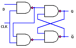 |
In the D latch, when the CLK input is logic 1, the Q output will always
reflect the logic level present at the D input, no matter how that changes.
When the CLK input falls to logic 0, the last state of the D input is trapped
and held in the latch, for use by whatever other circuits may need this
signal.
Because the single D input is also inverted to provide the signal to reset the latch, this latch circuit cannot experience a "race" condition caused by all inputs being at logic 1 simultaneously. Therefore the D latch circuit can be safely used in any circuit.
|
Although the D latch does not have to be made edge triggered
for safe operation, there are some applications where an edge-triggered
D flip-flop is desirable. This can be accomplished by using a D latch circuit
as the master section of an RS flip-flop. Both types are useful, so both
are made commercially available.
Except for the change in input circuitry, a D flip-flop works
just like the RS flip-flop.
With all of these different types of latches and flip-flops, the logic diagrams we have been using have gotten rather large, especially for the edge-triggered flip-flops. Fortunately, it really isn't necessary to follow and understand the inner workings of any of these circuits when they are use in larger applications. Instead, we use a set of very simple symbols to represent each type of latch or flip-flop in larger logical circuits.