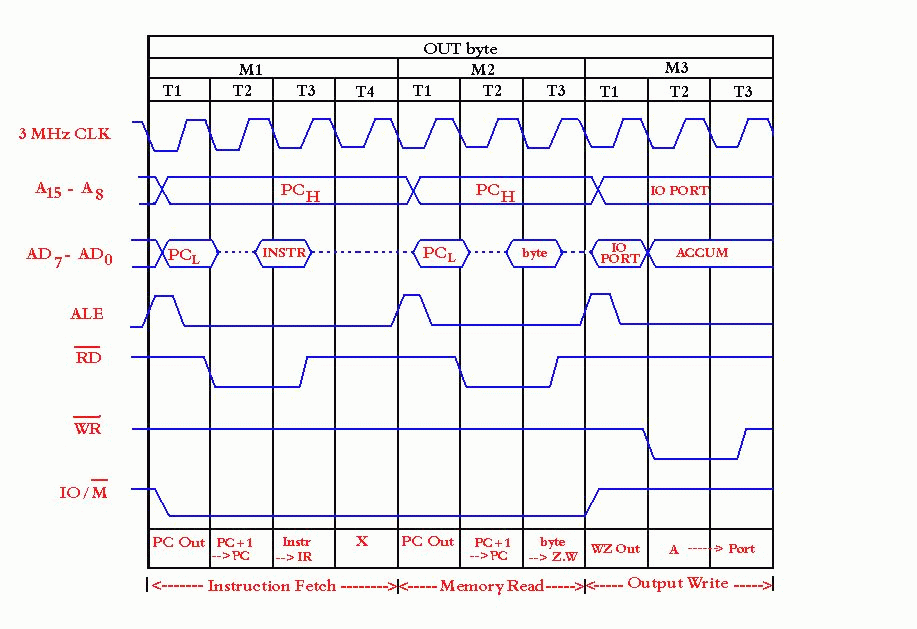
The above figure gives an example of 8085 timing, showing the value of external control signals. Of course, at the same time internal control signals are being generated by the control unit to control internal data transfers. Three machine cycles ( M1, M2, M3) are needed. During the first, the OUT instruction is fetched. The second machine cycle fetches the second half of the instruction, which contains the number of the I/O device selected for output. During the third cycle, the contents of the AC are written out to the selected device over the data bus.
The start of each machine cycle is signaled by the Address Latch Enabled (ALE) pulse from the control unit. The ALE pulse alerts external circuits. During timing state T1, of machine cycle M1, the control unit sets the Io/M signal to indicate that this is a memory operation. Also, the control unit causes the contents of the PC to be placed on the address bus (A15 - A8) and address/data bus (AD7 - AD0 ). With the falling edge of the ALE pulse, the other modules on the bus store the address.
During timing state T2, the addressed memory module places the contents of the addressed memory location on the address / data bus. The control unit sets the Read Control (RD) signal to indicate a read, but it waits until T3 to copy the data from the bus. This gives the memory module time to put the data on the bus and for the signal levels to stabilize. The final state, T4, is a bus idle state during which the CPU decodes the instruction. The remaining machine cycle proceed in a similar fashion.